
The Trillion-Dollar Question Behind Every Chip
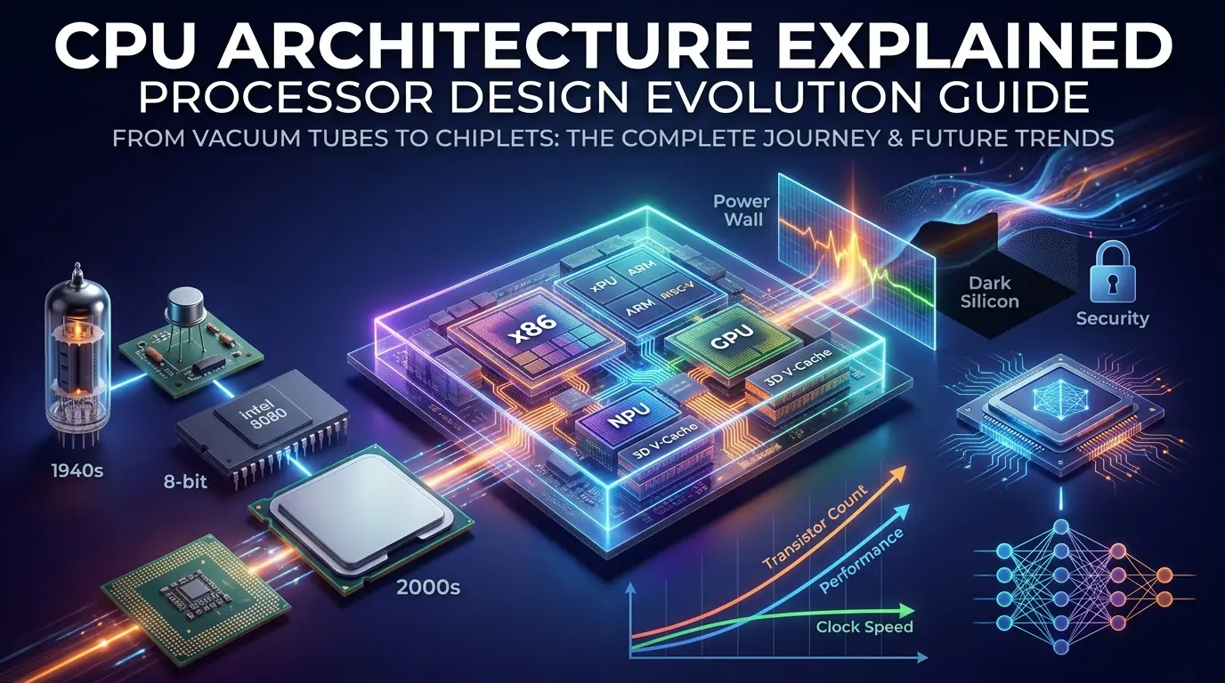
In 1971, Intel released a chip the size of a thumbnail. It had 2,300 transistors, operated at 740 kHz, and cost roughly five dollars in today’s money. The company called it “a new era in integrated electronics.” Fifty-three years later, Apple’s M3 processor contains 25 billion transistors, roughly a ten-million-fold increase.
But here is what most articles on CPU architecture quietly get wrong: performance today is no longer primarily about transistor count.

The real story is far more complex, and far more interesting. Modern processor design is a balancing act between physics, mathematics, economics, and geopolitics. Thermal limits constrain how fast chips can run. Security vulnerabilities undermine the very optimizations that make processors fast. Open-source instruction sets are reshaping the global semiconductor industry in ways that have little to do with logic gates.
This guide covers all of it. From foundational principles of how processors work, to the architectural battle between x86 and ARM, to the emerging threats quietly redefining what “performance” even means, this is the CPU architecture guide that existing content consistently fails to deliver.
- How CPUs evolved from vacuum tubes to chiplets, and why the path matters
- The real difference between ISA, microarchitecture, and why most people confuse them
- Why RISC and CISC are no longer opposites in modern processor design
- How out-of-order execution recovers hundreds of wasted pipeline cycles
- Why the Power Wall, not Moore’s Law, is the defining constraint of 2026
- Quantitative comparison of ARM vs. x86 efficiency with real benchmark data
- Why RISC-V is as much a geopolitical instrument as a technical specification
- The security crisis embedded inside speculative execution, and why it is unfixable
- How chiplets and 3D stacking are redefining what a “processor” even is
What Is CPU Architecture? Defining the Two Concepts Most People Conflate
Before exploring how processors evolved, it is essential to establish precise definitions. The term “CPU architecture” is routinely used to mean two distinct things, and conflating them leads to systematic confusion when reading vendor documentation, benchmark reports, or hardware reviews.

Definition 1: Instruction Set Architecture (ISA)
The instruction set architecture is the contract between software and hardware. It defines the complete vocabulary of operations a processor can perform, every legal instruction, its binary encoding, the registers available to software, memory addressing rules, and how the chip handles exceptions.
When a developer writes code in C++, Python, or any compiled language, a compiler translates that human-readable logic into binary instructions drawn entirely from this vocabulary.
Different processor families speak different dialects. Intel and AMD processors use x86, a CISC-oriented ISA originating in 1978. Nearly every smartphone uses ARM, a RISC-based ISA developed at Acorn Computers in the 1980s. An increasingly consequential third option, RISC-V, is a completely open-source ISA with no licensing fees, designed at the University of California, Berkeley in 2010.
The ISA defines what a processor does. It says nothing about how the hardware accomplishes it.
Definition 2: Microarchitecture
Microarchitecture is the actual hardware implementation of the ISA, the pipelines, execution units, caches, branch predictors, and control logic that carry out instructions. Two processors can share an identical ISA while having completely different microarchitectures. AMD’s Zen 5 and Intel’s Arrow Lake both execute x86-64 instructions, but their internal pipeline depths, cache configurations, execution unit counts, and power management strategies differ significantly.
When Intel or AMD release a “new generation” processor without changing the ISA, what changes is the microarchitecture. This distinction matters for software developers, system architects, and anyone evaluating performance claims.
The Architectural Foundation: Von Neumann vs. Harvard
Virtually every general-purpose computer built since the 1940s follows the von Neumann architecture, proposed by mathematician John von Neumann. Its defining feature is a single, unified memory space that holds both program instructions and the data those programs operate on. The CPU fetches an instruction, decodes it, executes the operation, and repeats indefinitely.
The Harvard architecture, by contrast, uses physically separate memory systems for instructions and data, allowing the CPU to fetch an instruction and access data simultaneously, eliminating the bottleneck caused by competing for a shared bus. Modern processors use a hybrid: separate instruction and data caches at the hardware level, backed by unified main memory. This provides Harvard-style parallelism in the fast path while retaining the flexibility of a unified address space for software.
Key takeaway: The ISA defines what a processor can do; the microarchitecture defines how it does it. Understanding this distinction is the prerequisite for everything else in processor design.
From Vacuum Tubes to Silicon: The History That Built Modern Processors
The semiconductor revolution began on December 23, 1947, at Bell Laboratories. John Bardeen and Walter Brattain demonstrated the first point-contact transistor using a germanium substrate, a solid-state device capable of amplifying electrical signals without the fragility, heat, or size of vacuum tubes. William Shockley formalized the theoretical model of the junction transistor in 1948, work for which all three would share the Nobel Prize in Physics.

Silicon replaced germanium as the preferred substrate by the mid-1950s, driven by silicon’s superior thermal stability. Germanium’s high susceptibility to leakage current at elevated temperatures made it unreliable in real operating conditions. The development of zone refining techniques by William Pfann and Henry Theurer produced the ultra-pure silicon substrates necessary for consistent device fabrication, while photolithographic patterning allowed microscopic geometric structures to be transferred onto wafers with repeatable precision.
In 1958, Jack Kilby at Texas Instruments demonstrated the first integrated circuit, proving that resistors, capacitors, and transistors could all be fabricated from a single semiconductor substrate, eliminating the need for manual wiring. Robert Noyce at Fairchild Semiconductor independently developed the planar process in 1959, enabling aluminum interconnects to be deposited directly onto a flat, oxide-protected silicon surface. This was the technique that made mass production of integrated circuits practical and economically viable.
The logical endpoint arrived in 1971. Intel’s 4004 — a 4-bit processor fabricated on a 10-micron process with 2,250 transistors, became the world’s first commercial single-chip microprocessor. It executed between 46,000 and 92,000 instructions per second. ENIAC, built just 25 years earlier to fill an entire room at a cost equivalent to $5.5 million today, achieved only 5,000 instructions per second. The microprocessor era had begun.
By 1974, 8-bit designs like the Intel 8080 (6,000 transistors on a 6-micron NMOS process), the Motorola 6800, and the MOS Technology 6502 had established architectures capable of driving personal computers. The IBM PC, launched in 1981 with Intel’s 8088, locked in x86 as the dominant PC architecture, a consequence that would shape the industry for the next four decades.
How a CPU Executes Instructions: The Fetch-Decode-Execute Cycle
Every CPU, from the simplest microcontroller to the most powerful server chip, operates through a repeating loop called the instruction cycle. Grasping this cycle is the prerequisite for understanding pipelining, out-of-order execution, and every other performance optimization built on top of it.

Stage 1: Fetch
The program counter register holds the memory address of the next instruction to execute. The control unit sends this address to memory, retrieves the instruction, loads it into the instruction register, and increments the program counter to point at the following instruction.
On older processors, this was a slow round-trip to external RAM. On modern processors, the instruction cache intercepts nearly all fetches, delivering instructions in one or two clock cycles.
Stage 2: Decode
The control unit breaks the fetched instruction into its component parts. Every instruction contains an opcode, a binary code identifying the specific operation, and operands specifying the data sources and destination.
An instruction like “ADD R1, R2” tells the processor to add the values in registers R1 and R2 and store the result. The decoder translates the binary encoding into control signals that configure the execution hardware.
Stage 3: Execute
With the instruction decoded, the relevant unit activates. Arithmetic and logical operations (addition, subtraction, comparison, bitwise AND/OR/XOR) execute in the Arithmetic Logic Unit. Memory operations travel to the Load/Store Unit, which manages data transfers between the register file and cache hierarchy. Branch instructions may update the program counter, redirecting execution flow.
Stages 4 and 5: Memory Access and Write-Back
If the instruction reads from or writes to memory, that transfer occurs in the memory stage. The final result is committed to the register file in the write-back stage. These last two stages execute only when the instruction requires them, an ALU operation between two registers skips the memory stage entirely.
The power of this pipeline comes from overlapping stages. While one instruction is executing, the next is being decoded, and the one after that is being fetched. This overlap, pipelining, is why a processor does not need to complete each instruction fully before beginning the next one. In an ideal pipeline, one instruction completes every clock cycle.
Real workloads introduce hazards that disrupt this ideal: data dependencies between consecutive instructions, structural conflicts when multiple instructions need the same hardware unit, and control hazards when branch instructions redirect the instruction stream before the pipeline can respond. Managing these hazards is what separates simple processor designs from high-performance ones.
Key takeaway: The fetch-decode-execute cycle is the universal operating principle of every CPU ever built. Every advanced technique in processor design, pipelining, superscalar execution, branch prediction, is an optimization layered on top of this fundamental loop.
RISC vs. CISC: The Philosophical Split That Still Shapes Every Chip
The late 1970s saw a fundamental disagreement among computer scientists about what processors should be optimized for. That debate produced two design philosophies that defined the next four decades of processor development.

The CISC Approach
Complex Instruction Set Computer designs, exemplified by Intel’s x86 family, pack tremendous capability into individual instructions. A single x86 instruction can load a value from memory, perform arithmetic, and write the result back, operations that would require three separate instructions in a simpler design. Instructions vary in length from one to fifteen bytes, a consequence of encoding so much functionality.
This approach made excellent sense in the late 1970s, when memory was both slow and expensive. Compact programs with information-dense instructions minimized memory usage and reduced the frequency of slow memory accesses. The complexity was managed through microcode, firmware that translated high-level instructions into simpler internal operations.
The costs were real: variable-length instructions make decoding difficult, hardware complexity adds power consumption, and microcode translation adds latency. But when memory was the bottleneck, dense instructions were worth those costs.
The RISC Approach
Research at UC Berkeley’s RISC project under David Patterson, and simultaneously at Stanford’s MIPS project under John Hennessy, revealed a surprising finding: typical programs use only a small, simple subset of a CISC processor’s instruction set. The vast majority of clock cycles were spent on simple loads, stores, arithmetic, and branches, not the complex multi-step operations that CISC was designed to encode efficiently.
Reduced Instruction Set Computer designs eliminated the complexity. Fixed-length, 32-bit instructions made decoding trivial and predictable. A strict load-store model required data to be explicitly moved into registers before computation, then explicitly stored back. All computation happened in a large general-purpose register file. The classic five-stage RISC pipeline could proceed without the irregular decode latencies that plagued CISC designs.
The results were striking. Berkeley’s RISC-I prototype, with just 44,420 transistors, outperformed the DEC VAX mainframe at common workloads. RISC-II, with 40,760 transistors and released in 1983, ran more than three times faster than its predecessor. The simplicity translated directly into performance.
The Modern Convergence
Here is the insight most introductory articles skip: the distinction between RISC and CISC has largely dissolved at the implementation level.
Modern x86 processors from Intel and AMD decode complex x86 instructions into simpler, uniform internal operations called micro-operations (µops) before execution. These µops flow through what is effectively a RISC-style pipeline, with register renaming, out-of-order scheduling, and superscalar issues. The x86 ISA is the external interface, the language software speaks. The internal execution engine is RISC.
Conversely, modern ARM processors have adopted features once associated with CISC: rich vector instruction sets like NEON and SVE2, deep out-of-order pipelines, and hardware speculative execution. The RISC label describes the design philosophy, not the feature set.
The competition today is not RISC versus CISC. It is between different microarchitectural approaches to maximizing instruction throughput per watt.
The x86 Evolution: How a 1978 Design Survived to 2026
Intel’s 8086, released in 1978, introduced the x86 architecture. Its selection for the original IBM PC in 1981 was the pivotal event, once software developers targeted x86, the economic incentives to maintain backward compatibility became overwhelming. Every subsequent generation had to run every program ever written for the previous one.
| Generation | Year | Key Innovation | Transistors | Memory Limit |
|---|---|---|---|---|
| Intel 8086 | 1978 | Foundational 16-bit x86; segmented memory model | 29,000 | 1 MB |
| Intel 80286 | 1982 | Protected mode; hardware multitasking support | 134,000 | 16 MB |
| Intel 80386 | 1985 | Full 32-bit transition; integrated MMU and paging | 275,000 | 4 GB (virtual) |
| Intel 80486 | 1989 | On-chip FPU; 8 KB L1 cache; pipelined execution | 1,200,000 | 4 GB |
| Pentium (P5) | 1993 | Superscalar dual pipelines; dynamic branch prediction | 3,100,000 | 4 GB |
| Pentium Pro (P6) | 1995 | Out-of-order execution; µop decoding; ROB introduced | 5,500,000 | 64 GB (PAE) |
The Pentium Pro’s P6 microarchitecture is the direct ancestor of every modern Intel design. Its core innovation, translating complex x86 instructions into simpler µops, then executing those µops out of program order through a Reorder Buffer, remains the fundamental approach Intel uses today.
AMD’s Zen architecture follows the same paradigm. AMD extended x86 to 64 bits in 2003 with AMD64, doubling the general-purpose register count from 8 to 16. Intel, having failed with its Itanium alternative, adopted AMD’s extension and rebranded it x86-64.
Out-of-Order Execution: The Engineering That Hides Latency
The most significant microarchitectural innovation in processor design is out-of-order execution. To understand why it matters, start with the problem it solves.

In a simple in-order pipeline, instructions execute in strict program sequence. If instruction 3 stalls waiting for data that instruction 2 has not finished computing, or worse, waiting for a cache miss that takes 100 cycles to resolve, the entire pipeline stops. Every subsequent instruction queues behind the stall, idle, while the processor waits.
Out-of-order execution breaks this constraint. The processor examines a window of upcoming instructions, identifies which ones have all their inputs already available, and executes those immediately, regardless of their position in the original program sequence. Stalled instructions wait in a holding structure called a reservation station until their operands arrive.
Several key hardware structures make this possible:
- Register Alias Table (RAT): Maps software-visible architectural registers to a larger pool of physical registers. This eliminates false read-after-write and write-after-write dependencies that would otherwise prevent reordering, allowing more instructions to execute in parallel.
- Reservation Stations: Hold in-flight µops, tracking whether each source operand has been computed yet. Each station broadcasts a tag identifying which instruction will produce its needed value, and receives results via the Common Data Bus when execution completes.
- Reorder Buffer (ROB): Tracks all in-flight instructions in original program order, allowing results to be committed to the architectural register file sequentially even though execution occurred out of sequence. This ensures precise exception handling — if an exception occurs, the processor knows exactly which instructions had completed.
The performance advantage is measurable. Under controlled benchmarking with identical instruction sets and manufacturing nodes, an out-of-order RISC-V C910 core achieved a mean Instructions Per Cycle (IPC) of 1.61, a 119.5% improvement over a comparable dual-issue in-order design. Out-of-order processors routinely sustain multiple instructions completed per clock cycle because they exploit instruction-level parallelism hidden within what appears to be sequential code.
Branch Prediction: Keeping the Pipeline Full Through Uncertainty
Deep pipelines create a fundamental vulnerability. Conditional branch instructions, the if-statements and loops that give programs decision-making capability, require the processor to determine which of two paths to take. But evaluating that condition takes several pipeline stages. Rather than stall and wait, modern processors predict the outcome and speculatively execute instructions along the predicted path.
A wrong prediction means flushing speculatively-executed instructions from the pipeline and restarting from the correct branch target. In a deep, wide-issue pipeline, a single misprediction can waste fifteen to twenty clock cycles. At 5 GHz, that is three to four nanoseconds per misprediction, insignificant individually, but devastating at the frequency modern code encounters branches.
Modern CPUs implement a multi-tiered prediction hierarchy:
- Branch Target Buffer (BTB): Operates in the fetch stage with zero-cycle latency. Predicts the next program counter target from a table of recently observed branch outcomes.
- Gshare Predictor: Operates in the decode stage with one-cycle latency. Indexes a table of two-bit saturating counters using a global history register XORed with the program counter, capturing correlations between recent branches.
- TAGE Predictor: A tagged predictor using geometrically increasing history lengths. Resolves complex, correlated branch patterns that shorter-history predictors miss, using 3-bit prediction counters and 2-bit “useful” counters to manage table eviction.
The average misprediction penalty across this tiered hierarchy follows a precise mathematical relationship:
With default values representing a well-tuned modern predictor (BTB accuracy of 0.95), the penalty falls to roughly 1.1 cycles, dramatically better than the 4-cycle penalty of a naive, single-stage predictor. Standard bimodal predictors resolve approximately 93% of branches correctly across SPEC benchmarks.
Tournament predictors, which dynamically select between local and global history tables, add roughly 2% additional accuracy. Each percentage point of accuracy directly translates into pipeline throughput.
The Power Wall: Why Clock Speed Is No Longer the Lever It Was
For three decades, processor performance scaled reliably with each new generation of manufacturing. This was the era of Dennard Scaling, named after IBM engineer Robert Dennard. His observation was precise: as transistors shrink, their power density remains constant.
Smaller transistors switch faster and consume less power, allowing designers to simultaneously increase transistor density and raise clock frequencies without increasing total power consumption. The formula governing dynamic power in CMOS circuits is:
Dennard Scaling broke down around 2005, at sub-65 nanometer process nodes. As gate oxide layers reached atomic thicknesses, quantum mechanical tunneling allowed electrons to leak through even when transistors were “off.”
Leakage current grew exponentially, from negligible to a power component rivaling the dynamic term. To limit leakage, designers could no longer reduce operating voltage proportionally with transistor size. Voltage stalled at approximately 1.0 volt.
The result is the Power Wall. With transistor density still doubling each generation but voltage no longer decreasing, total chip power began rising rather than remaining constant. A fixed silicon die area can only dissipate so much heat. The consequence is Dark Silicon: large portions of a chip’s transistors must remain powered down, or run at reduced frequencies, at any given moment, because activating all of them simultaneously would exceed the chip’s Thermal Design Power (TDP).
This physical reality directly limits what adding more CPU cores can accomplish, a constraint formalized by Amdahl’s Law.
Amdahl's Law demonstrates that even a program that is 90% parallelizable reaches a maximum speedup of just 10× with unlimited cores, because the 10% serial fraction creates an absolute ceiling.
The dark silicon problem amplifies this: idle cores still consume thermal headroom, limiting what can run simultaneously. This mathematical and physical combination forced the transition from symmetric multi-core designs to heterogeneous architectures, mixing different core types and specialized accelerators, each optimized for specific tasks within a shared thermal budget.
Key takeaway: The end of Dennard Scaling is the most consequential event in CPU history since the integrated circuit. It transformed processor design from a frequency race into a system-level optimization problem spanning energy, security, and specialization.
The Rise of Specialized AI Accelerators: Moving Beyond General-Purpose Logic
The end of Dennard Scaling and the onset of the Power Wall forced a pivot away from "one-size-fits-all" general-purpose CPU cores. In 2026, the most significant driver of architectural change is not raw CPU clock speed, but the integration of specialized silicon designed specifically for the massive matrix multiplication operations that define modern AI.

The Fundamental Mismatch
General-purpose CPUs (the cores we have discussed thus far) are designed for branchy, serial-heavy code. They excel at making rapid decisions (if-then-else logic) and handling unpredictable data streams. However, neural network inference and training are the exact opposite: they are highly predictable, parallel, and mathematically dense.
Using a general-purpose CPU to perform AI inference is akin to using a sports car to transport a thousand shipping containers, it is technically possible, but monumentally inefficient. The energy cost of fetching an instruction, decoding it, and moving data across the CPU's complex cache hierarchy for a simple multiply-accumulate (MAC) operation is orders of magnitude higher than the cost of the math itself.
The Specialized Solution: NPU/TPU Architecture
Neural Processing Units (NPUs) and Tensor Processing Units (TPUs) discard the overhead of a general-purpose CPU. They feature:
- Systolic Arrays: Instead of a complex pipeline, these chips use a grid of simple processing elements that pass data directly to their neighbors. This minimizes memory movement, the most energy-expensive part of computing.
- Reduced Precision Arithmetic: While a CPU typically operates at 64-bit or 32-bit floating-point precision, NPUs aggressively use INT8 or FP8 precision. This allows for massive throughput, as smaller numbers require fewer transistors and consume significantly less power.
- Data-Flow Scheduling: Instead of a program counter fetching instructions one by one, AI accelerators use data-flow architectures where the chip is "configured" for a specific neural network layer, and data flows through the hardware like water through a pipe.
The "Heterogeneous" Reality
In 2026, the "CPU" is no longer a standalone component; it is an orchestrator. The modern processor is a Heterogeneous System on a Chip (SoC). The general-purpose cores handle the operating system and user interface, while the NPU handles the AI background tasks, and the GPU handles high-throughput vector graphics.
The architectural battleground of 2026 is no longer just about who has the fastest "CPU." It is about who has the most efficient AI-to-CPU offload pipeline. If a system can offload a background task to the NPU, it saves the CPU’s thermal budget for latency-critical tasks, extending battery life and sustaining higher performance under heavy workloads.
ARM vs. x86 in 2026: What the Benchmark Data Actually Shows
The conventional framing of ARM versus x86, mobile versus desktop, efficiency versus performance, has collapsed. Apple demonstrated with its M-series chips that ARM can not only compete with x86 in laptops and desktops, but surpass it on most workloads while consuming dramatically less power.
The numbers from direct architectural comparison tell a precise story. Testing the Apple M3 (ARMv8.6-A on TSMC's 3nm process) against the AMD Ryzen 7 3750H (x86-64 Zen+ on TSMC's 12nm process) under identical workloads reveals consistent patterns:
| Metric | Apple M3 (ARM) | AMD Ryzen 7 3750H (x86) |
|---|---|---|
| Process Node | TSMC 3 nm | TSMC 12 nm |
| IPC — Fibonacci | 3.74 | 2.49 |
| IPC — Matrix Multiply | 5.43 | 2.83 |
| Branch Misprediction Rate | 0.00067% | 0.095% |
| L1D Cache Miss Rate | 0.00046% | 0.0015% |
| Energy — Fibonacci (nJ/call) | 1.58 | 9.21 |
| Energy — Matrix Multiply (nJ/op) | 0.840 | 5.36 |
| Energy Efficiency Advantage (M3) | 5.82× better (Fibonacci) — 6.38× better (Matrix Multiply) | |
The M3's efficiency advantage stems from a combination of factors. Its higher IPC means it completes more useful work per clock cycle, reducing the total number of cycles, and thus total energy, required.
Its branch misprediction rate is approximately 140 times lower, eliminating the pipeline flush overhead that x86 processors pay more frequently. Its lower L1 cache miss rate means the core rarely stalls waiting for data, keeping the execution engine fed.
The economic implications are visible in cloud pricing. ARM-based AWS Graviton 3 instances cost $0.136 per hour for 4 vCPUs, compared to $0.178 for equivalent Intel Xeon instances, a 31% premium for x86. Scaled across 100 instances, this difference amounts to approximately $3,700 per month, or $44,400 annually. This cost differential is accelerating enterprise migration to ARM-based cloud infrastructure.

x86 retains meaningful advantages in specific domains. Single-threaded performance at high clock frequencies, reaching 5.8 GHz in current consumer desktop chips, remains important for gaming engines and other latency-critical applications.
Legacy software compatibility is significant for enterprises with decades of x86-compiled workloads. And NVIDIA's CUDA ecosystem, which dominates AI training, remains deeply integrated with x86 host systems.
ARM's relaxed memory consistency model also provides server-side advantages. Where x86 enforces strict memory ordering across all cores, requiring pipeline synchronization that limits throughput in highly concurrent workloads, ARM's relaxed model allows more aggressive hardware reordering. For database systems handling high volumes of concurrent transactions, this architectural choice often translates into measurable throughput gains.
RISC-V: Open-Source, Modular, and Geopolitically Strategic

RISC-V is not simply another processor architecture. It represents a different model for how computing infrastructure is built, owned, and controlled.
Developed at UC Berkeley and now governed by RISC-V International, RISC-V is released under permissive open-source licenses. Anyone can design, manufacture, and sell RISC-V processors without paying royalties or seeking permission. This contrasts sharply with ARM, which charges licensing fees and royalties for every implementation, and x86, which Intel and AMD license to very few parties under tightly controlled terms.
The architecture's modularity is a deliberate design philosophy. A small, frozen base integer ISA (RV32I for 32-bit systems, RV64I for 64-bit) provides the minimum instruction set needed for general-purpose software. Optional standard extensions add capabilities as needed without bloating implementations that do not require them:
- M: Hardware integer multiply and divide
- A: Atomic memory operations for multi-core synchronization
- F/D: Single and double precision floating-point
- C: 16-bit compressed encodings, reducing code size and instruction cache pressure
- V: Vector processing for parallel data operations
- G: The combination of I, M, A, F, and D, sufficient to run a general-purpose operating system
The RVA23 profile, the current standard for high-performance RISC-V, promotes the Vector extension from optional to mandatory, standardizing vector execution across compliant processors and enabling consistent software optimization.
What most coverage misses is the geopolitical dimension. Countries and companies that depend on ARM or x86 face exposure to export controls, licensing revocations, and supply-chain decisions made by entities outside their control. RISC-V eliminates these chokepoints.
According to industry analysis, over 21 billion RISC-V chips are projected to ship by 2031, with adoption already running approximately 25% ahead of earlier forecasts. Google's OpenTitan security chip, deployed in commercial Chromebooks, uses RISC-V. NVIDIA's Blackwell GPUs incorporate a RISC-V processor for internal management functions.
The instruction set has become strategic infrastructure, not just a technical specification.
Chiplets, 3D Stacking, and the Post-Monolithic Era
As lithographic scaling approaches physical limits, manufacturing a single large die on a cutting-edge process node has become economically unsustainable. Defects in silicon are random, they occur with a certain probability per unit area. Large dies have more area, so they statistically accumulate more defects. A single defect on a complex monolithic chip destroys the entire device, yielding losses that rise sharply with die size.

The chiplet paradigm solves this by decomposing a large SoC into smaller, specialized tiles. Each chiplet is fabricated separately on the process node best suited to its function.
High-performance CPU cores go on expensive 3nm silicon. Memory controllers and analog I/O components, which do not benefit from leading-edge nodes, go on mature 14nm or 28nm processes where analog circuits actually perform better. These individually tested "known good dies" are then assembled on a shared package.
Connecting separate dies requires standardized interconnects. The Universal Chiplet Interconnect Express (UCIe) standard defines a three-layer communication protocol, physical, die-to-die adapter, and protocol layers, that enables chiplets from different manufacturers to communicate using a common interface.
UCIe supports both micro-bump connections (20–55 µm pitch) and hybrid bonding, which establishes direct copper-to-copper molecular bonds capable of scaling interconnect pitch down to 700 nanometers, or 400 nm in development, orders of magnitude finer than any conventional package interconnect.
3D stacking extends integration vertically. AMD's 3D V-Cache technology stacks additional SRAM cache directly on top of compute chiplets using hybrid bonding, tripling L3 cache capacity without increasing the package footprint. The performance benefits for cache-sensitive workloads are substantial and well-documented: in gaming workloads, additional cache often matters more than additional core count or clock frequency.
Vertical stacking introduces significant engineering challenges. Heat generated by stacked dies cannot escape downward through the package, it must dissipate upward through the stack, creating concentrated thermal hotspots.
Different materials in the assembly expand at different rates under thermal cycling, generating mechanical stress that accumulates over millions of power cycles and can cause micro-cracking or delamination of bonding interfaces.
An additional challenge specific to advanced packaging is backside power delivery. Traditional chips route both signal wires and power distribution through the same layered metal stack on the front surface of the wafer. Backside Power Delivery Networks (BSPDNs) move the heavy power grid to the back of the silicon substrate, reducing resistance losses and freeing the front surface for signal routing.
The tradeoff is diagnostic: a thick metal plane on the wafer's back surface blocks the physical access needed for Focused Ion Beam (FIB) failure analysis, making debugging substantially harder.
Key takeaway: Chiplets represent a fundamental shift from "design the best possible single die" to "design the best possible system of interconnected tiles." The packaging has become a core component of the processor architecture, not a housing around it.
The Speculative Execution Security Crisis: An Architectural Paradigm Failure
Most coverage of the Spectre and Meltdown vulnerabilities, disclosed in January 2018, frames them as security bugs, serious, but patchable. This framing misses the deeper significance.

Spectre and Meltdown revealed that speculative execution creates information leakage that cannot be fully contained within the ISA's abstract computational model. When a processor speculatively executes instructions down a predicted branch path that ultimately proves incorrect, those instructions leave measurable traces in the microarchitecture, in cache line occupancy states, branch predictor table entries, execution port timing, even after the speculative results are discarded and the pipeline is flushed.
An attacker who can measure these traces can infer information from memory they were never authorized to access, including kernel memory, hypervisor data, and in cloud environments, data belonging to other tenants on the same physical host.
As documented in the original Spectre research, this vulnerability affected Intel, AMD, and ARM processors simultaneously, affecting billions of devices across the industry. Subsequent research identified hundreds of exploitable code sequences within standard libraries including glibc alone. Later variants demonstrated practical cross-virtual-machine leakage in modern cloud environments.
The critical insight is that this is not a bug class. It is an architectural paradigm failure. The assumption underlying out-of-order design, that speculatively executed instructions are architecturally invisible if rolled back, leaving no trace the software abstraction layer must account for, was false.
That assumption was never formally modeled as a security property during the decades these architectures were designed and refined.
The mitigations required to address speculative execution vulnerabilities directly degrade performance. Flushing branch predictors at privilege boundaries, inserting serializing instructions, isolating page tables, and reducing speculation depth all constrain the exact optimizations that justify the complexity of modern out-of-order processors. Security patches quietly erased a portion of each generation's performance gains, though vendors rarely report "security-adjusted performance" in their marketing materials.
This creates a structural antagonism between performance and security that cannot be fully resolved within the current architectural paradigm. Future processor designs may need to fundamentally reconsider how aggressive speculation interacts with security isolation, possibly accepting reduced speculation depth in exchange for verifiable security boundaries.
Selectively partitioned branch predictors and hardware-enforced speculation limits are active areas of research at major processor manufacturers and in the academic community documented by IEEE Xplore.
Before and After: What Out-of-Order Execution Actually Delivers
A concrete example makes the performance impact of out-of-order execution tangible.

Before: In-Order Pipeline
Consider three consecutive instructions: load a value from memory (cache miss, 100-cycle latency), add a constant to that loaded value, then multiply two completely unrelated registers.
In an in-order pipeline: the load issues, triggers a cache miss, and the pipeline stalls for 100 cycles. The add instruction waits, it cannot proceed until the load completes, since it needs the loaded value. The multiply instruction also waits, even though it has no dependency on the load or add whatsoever. Total: approximately 102 cycles for three instructions. Effective utilization: roughly 3%.
After: Out-of-Order Pipeline
The same three instructions in an out-of-order processor: the load issues and waits in a reservation station for its cache miss to resolve. Meanwhile, the processor examines the multiply instruction, recognizes that its operands are already available in registers, and executes it immediately, during the cache miss wait. When the load completes after 100 cycles, the add executes. The multiple result was computed "for free" during the stall.
Total effective cycles: approximately 101. The multiply completed during the wait, recovering nearly all the lost throughput. An operation that would have taken 102 cycles sequentially now effectively took 101 cycles while completing all three instructions. This is the core value proposition of out-of-order execution: it hides latency by exploiting instruction-level parallelism that is invisible to the programmer but real in the instruction stream.
Five Common Mistakes in Understanding and Evaluating CPUs

Mistake 1: Using clock speed as the primary performance comparison
Clock frequency is one variable among many. A processor at 3 GHz with high IPC, a deep cache hierarchy, and an efficient branch predictor will consistently outperform a 5 GHz processor that stalls frequently on cache misses or mispredicted branches. The Apple M3's superior IPC is precisely why it often matches or exceeds higher-clocked x86 chips while consuming a fraction of the energy.
Mistake 2: Assuming more cores always improve performance
Amdahl's Law makes this precise. Programs with significant serial sections gain little from additional cores because the serial portion creates a hard ceiling on total speedup. A gaming workload dominated by a single main thread benefits far more from higher per-core performance and cache capacity than from doubling core count. Buying more cores for a serial workload wastes thermal budget and money.
Mistake 3: Treating published benchmarks as real-world performance
Most benchmark results are reported without specifying which speculative execution mitigations are enabled or under what thermal conditions the test ran. "Security-adjusted performance", which accounts for the overhead of required patches, and "sustained performance", which accounts for thermal throttling under continuous load, can differ significantly from peak benchmark numbers.
Mistake 4: Dismissing RISC-V as experimental
RISC-V has shipped in production hardware from Google, NVIDIA, Western Digital, Qualcomm, and others. The RVA23 profile provides the software portability guarantee that enterprise adoption requires. The software ecosystem is still maturing, but the architecture is production-ready for a growing range of workloads, and its geopolitical advantages are driving adoption independent of pure technical merit.
Mistake 5: Ignoring the security-performance tradeoff
Every enterprise deploying CPUs in multi-tenant or security-sensitive environments must account for the performance cost of speculative execution mitigations. This cost is real, workload-dependent, and frequently omitted from vendor performance claims. Evaluating CPUs without accounting for this overhead produces misleading comparisons.
Future Directions: What Comes After the Current Architecture Era
The near-term trajectory of processor design reflects the convergence of several forces that have been building for years.

Security-aware speculation is becoming a design priority rather than a retrofit. Architectures will implement selective speculation with partitioned predictors that prevent cross-boundary information leakage, accepting measured performance reductions in exchange for verifiable security guarantees. The era of "speculate everything and patch the leaks" is ending.
Memory-centric computing addresses a bottleneck that becomes more visible as compute density increases. For AI inference and training workloads, among the most demanding loads placed on modern hardware, moving data between memory and compute units consumes more energy than the computation itself.
Near-memory computing places processing logic adjacent to or within memory arrays, dramatically reducing data movement costs. This represents a potential reorganization of the fundamental compute hierarchy.
AI-assisted chip design is already influencing floorplanning and physical routing. As machine learning tools demonstrate competitive results against human designers in specific optimization tasks, the prospect of architectures optimized beyond what engineers can fully reason about becomes real. This introduces new accountability questions: how do you audit a design if no engineer fully understands the optimization path that produced it?
The Bell Labs model of deep foundational research producing decade-spanning technological impact, the transistor in 1947 changed computing through 2024 and beyond, reminds us that the most important architectural innovations are often not predictable from the current trajectory.
RISC-V's emergence from an academic project into geopolitical infrastructure is one recent example. The next may be photonic interconnects, neuromorphic computing, or an architectural simplification so radical it forces a rethinking of the security-performance tradeoff at its root.
Conclusion: Architecture Is Now the Lever That Matters
The story of CPU architecture is often told as a linear march toward faster chips. The reality is richer, more constrained, and more consequential.
Dennard Scaling ended. The Power Wall created Dark Silicon. Speculative execution, the optimization that made modern performance possible, introduced security vulnerabilities that cannot be fully resolved within the existing paradigm. The transistor count on a single die can no longer be the primary measure of progress.
What replaced the era of monolithic frequency scaling is a more complex ecosystem: heterogeneous architectures combining multiple core types, specialized accelerators for AI and cryptography, chiplet-based designs that bypass manufacturing yield limits, and open ISAs that introduce sovereignty as a criterion alongside performance and efficiency.
The architects of tomorrow's processors must be conversant in physics, security theory, economics, and supply-chain dynamics, not just digital logic. The chip is no longer just a component. It is infrastructure. Understanding the architectural choices behind any given processor, not just its marketing headline, is the foundation for every informed decision about the systems built on top of it.
Stay updated, stay curious, and let architecture, not just marketing, drive your next CPU choice.


")


[…] Read the Full Article → […]
[…] Read the Full Article → […]